
As we discussed in “Boundary Scan/JTAG I“, Boundary scan testing is implemented using a JTAG controller. Boundary scan testing was built to test the interconnections between different chips, and JTAG plays a crucial role. Here, we are going to discuss how JTAG works. The components of a JTAG interface/controller are connected within a design as shown in Figure 1.

- TAP controller (Test Access Port) : This is a finite state machine which monitors the control signals. It is discussed in detail in next section.
- TAP interface signals: These are 5 signals names as TCK,TMS,TDI,TDO and TRST (TRST is optional)
- Registers: There are 2 kinds of registers – Data Registers and Instruction Registers. Instruction registers store the info of what instruction is going to be executed, while data registers are used to execute the instruction. Data registers can be Bypass register, Boundary Scan Register or Identification Register. The details of registers and the instructions they perform will be discussed later.
- Boundary Scan Cells: These are the interface between the chip ports and interface logic as we discussed in Boundary Scan/JTAG I.
The following points should be noted while referring to the connections shown in Figure 1.
- Only one register can be connected between TDI and TDO.
- The decision of which data register will be connected is derived from TAP FSM as it loads the instruction register first. Based on the decoded instruction, a particular data register (bypass/identification/boundary scan) is connected from TDI to TDO.
What is TAP controller?
Since TAP controls all the operations, understanding it is necessary before going further. TAP controller is a 16 state FSM responsible for driving the complete JTAG system.
The five important signals are as follows:
TCK : Provides clock for state transitions
TDI : Serial Data input
TDO : Serial Data output
TMS : A ‘Test mode select’ signal which helps to decide the next state.
TRST : Used to reset the FSM and is an optional signal.
Let us study the inputs/outputs of TAP FSM first. Figure 2 shows the IOs of FSM.

- FSM provides control signals to the design which are:
CaptureIR, ShiftIR, UpdateIR : For IR (Instruction) registers
CaptureDR, ShiftDR, UpdateDR : For data registers and general design
2. TDI and TDO are not the direct Input/Output of FSM . FSM only provides control signals to decide which register will be connected between TDI and TDO.
3. The ‘Select’ signal decides the output of TDO:
Select = 0 => Data Register output
Select = 1 => IR Register output
The state transition diagram of TAP FSM is given in Figure 3.
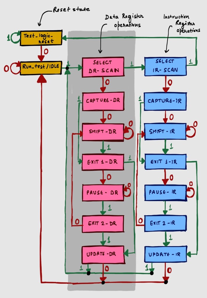
I would like to explain it gradually in simple steps. Let us first understand how to read the above FSM.
In the above figure, value shown by red and green arrows is TMS. TMS acts as one of the input, and other input is clock TCK. TMS is sampled on rising edge of TCK. There are 16 states which are traversed based on the value of TMS.
Example:
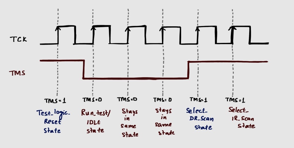
TAP FSM initialises in Test_Logic_Reset state. This is where TMS is at its default value (‘1’) and TCK starts clocking.
When TMS is pulled to ‘0’, FSM enters Run_Test/IDLE state.
If TMS stays ‘0’, this state is maintained. When TMS goes to ‘1’ , Select_DR_Scan state is reached.
When TMS stays ‘1’ for one more cycle, it reaches Select_IR_Scan state.
Depending on whether we want to operate on IR or Data register, we choose the required state. Now you can observe that the path for Capture/ Shift/ Exit/ Pause/ Update is same for both kind of registers.
This explains how we can read the FSM and how all 16 states of FSM can be reached. However, the details of these states will be discussed in next article.
Why TRST is optional?
TRST is an optional signal which is quite established till now. However, the reason can be understood easily from the FSM. Pick any state in Figure 3 and navigate the states by holding TMS ‘1’. In maximum of 5 TCK cycles, you will reach Test_Logic_Reset state. This means that the reset state (Test_Logic_Reset) can be achieved with a combination of TCK and TMS signals, so TRST signal is not always required.

Leave a reply to Anonymous Cancel reply