Category: Design For Test
-

Test-Points
We have discussed DFT and Scan basics in previous articles. Let us talk about another important DFT structure – Test points. The aim of DFT structures is to make the design controllable and observable. We have seen how scan chains allow us to control the design by passing test values, and observing the captured values.…
-
Boundary Scan/JTAG – III
Boundary Scan Registers Boundary scan testing consists of certain registers as mentioned in Boundary Scan-II. There are two kinds of registers: Instruction registers: As the name implies, this register stores the instructions which can be decoded and executed as per requirements. Data registers: Data registers are selected based on the decode instruction from the instruction…
-

Boundary Scan/JTAG – II
As we discussed in “Boundary Scan/JTAG I“, Boundary scan testing is implemented using a JTAG controller. Boundary scan testing was built to test the interconnections between different chips, and JTAG plays a crucial role. Here, we are going to discuss how JTAG works. The components of a JTAG interface/controller are connected within a design as…
-
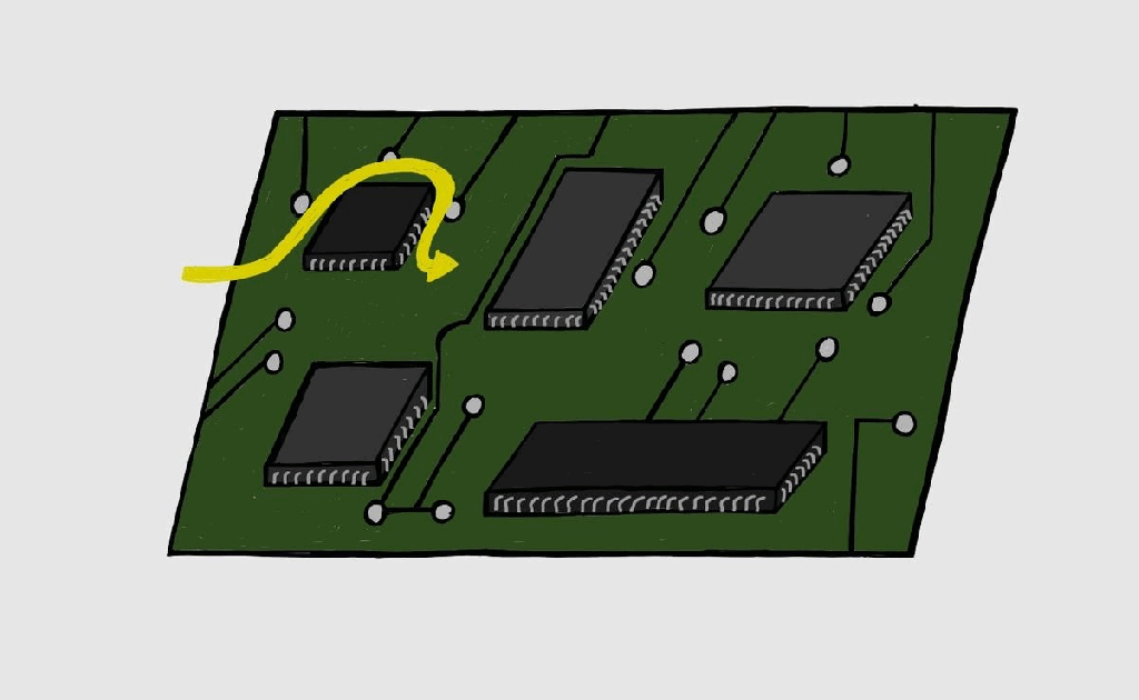
Boundary Scan/JTAG – I
A PCB (Printed Circuit Board) assembles a number of Integrated circuits and other electrical components. When such an assembly is created, testing the integration is also necessary. As the density of such boards increased and further miniaturisation happened, it became impossible to access all the nodes with physical probes. Hence, the boundary scan testing technique…
-
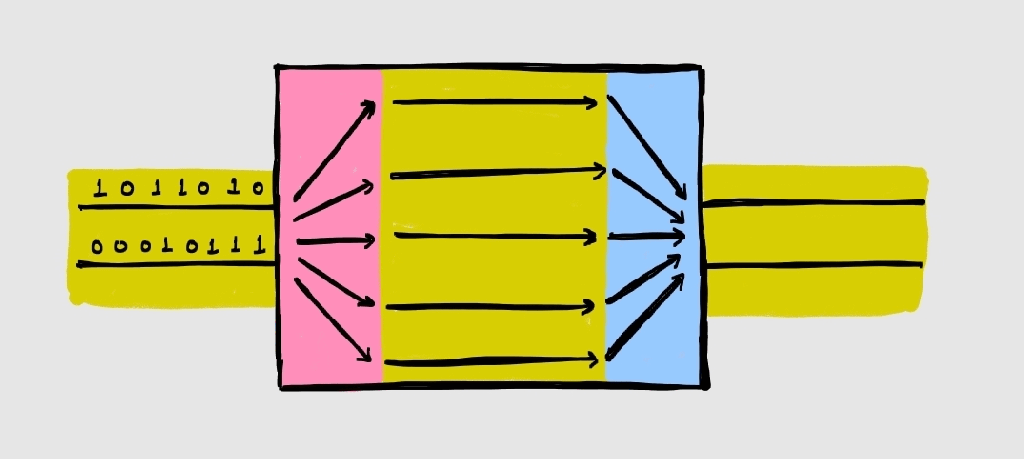
Scan Compression
Understanding scan operation is a pre-requisite to understand scan compression. My article “Scan and Resets” defines scan in simple terms. The basic concept of scan is to convert all flip flops in the design into scannable flipflops (having scan_in, scan_out and scan_enable) and connect them to form scan chains. Theoretically, there is no limit on…
-
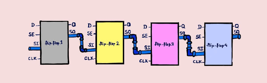
Scan And Resets
DFT – ‘Design for Test’ is an important task in modern chip designs. Basic DFT constitutes scan design. I have discussed fault models and ATPG testing in different articles. Before going deeper into other DFT topics, let us understand what a scan design is. When RTL design is coded and converted into gate netlist, the…
-
Wrapper Chains
The major part of DFT is converting a design into a scannable design where all the flip flops are connected in a network of scan chains. With more complex designs, and many scan chains to handle, hierarchical DFT comes into play. This methodology involves wrapper chain structure, which will be discussed here. Wrapper chains are…
-
ATPG – Stuck-at and At-speed
ATPG – Automatic test Pattern Generation Used to create a set of patterns, which can test the design for the faults as discussed in DFT-Fault models article. I would recommend reading DFT-Fault models to understand this article better. Has two main steps: Generate patterns, Perform fault simulation to check which faults can be detected by…
-
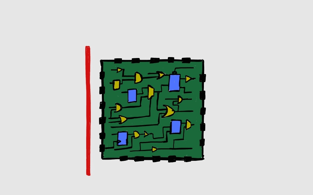
DFT – Fault Models
DFT – Design for test is a technique that helps to tests for manufacturing or structural defects. Unlike Functional verification, which tests for the bugs/issues in the functionality of the design, DFT works to test if fabrication induced any defect in the chip. Some of the techniques of DFT are Scan, BIST, JTAG etc. The…
