DFT – Design for test is a technique that helps to tests for manufacturing or structural defects. Unlike Functional verification, which tests for the bugs/issues in the functionality of the design, DFT works to test if fabrication induced any defect in the chip. Some of the techniques of DFT are Scan, BIST, JTAG etc. The test patterns generated before-hand by DFT engineers are run over a manufactured chip to detect some faults which we will be discussing in this article.
These faults can be categorized into three kinds: Functional, Current and Speed.
Functional :
These faults can be:
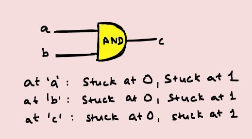
Stuck-at
The circuit node might get shorted to Vdd or GND, making the pin value stuck to 1 or 0.
For ‘n’ inputs, there can be 2(n+1) faults. For example:
Toggle
The circuit node should be able to toggle to both 0 and 1 values.
Functional tests used to detect above faults are most common DFT tests. It involves:
- Applying a pattern of 0s and 1s to the circuit
- Measure the values at the output (to check if matches the expected value).
Current :
These are the faults which can occur at transistor level and hence, need a different way of being tested. IDDQ testing involves sending a pattern, and measuring the excessive current to find out the defect. Generally, there is no static current path between VDD and GND (only leakage currents), but a defect might create such a path leading to an extra current flow. IDDQ tests measure these currents to detect the defect.
Some examples of faults tested by IDDQ tests are:
Bridge Faults
There are two CMOS circuits, where the two output wires (having opposite values) are close to each other. The bridging defect can cause a short between them, which creates a current path between VDD and GND. The potential at the short can go upto VDD/2 (worst case) and cause metastability at both output lines.

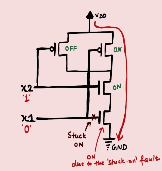
Stuck-on Faults
Consider a NAND gate circuit, where the input to nMOS is left ‘on’ as its gate is shorted to VDD (due to a defect). When x1 = 0 and x2 = 1, we expect an output of ‘1’ in a fault-free circuit, but due to the defect, there exists a path between VDD to GND and excessive current flows through the red path.
Speed :
This includes the faults which are detected by at-speed testing, such as transition delay faults and path delay faults.
Transition Delay Faults
- These are the faults across the gate terminals which leads to a slow transition from ‘o’ to ‘1’ or ‘1’ to ‘0’.
- Each pin is tested to detect these faults using a set of two patterns.
- Example: A 2-input AND gate will have 6 possible transition faults.
Path Delay Faults
- These are the cumulative faults along a specific path (between launch and capture point) which causes a slow transition of values.
- The tool needs an input of specific paths to check for these faults.
The detection of these faults needs a set of two patterns, as follows:
- Application of first vector to initialize the circuit
- Application of second vector to start the transition (0->1 or 1->0).
- Wait for the expected time
- Measure the values across observing points.
If the correct value appears at the observing points at the right time w.r.t the clock, the circuit is fault-free. If not, speed fault is detected.

Leave a reply to Anonymous Cancel reply