
We have discussed DFT and Scan basics in previous articles. Let us talk about another important DFT structure – Test points.
The aim of DFT structures is to make the design controllable and observable. We have seen how scan chains allow us to control the design by passing test values, and observing the captured values. When ATPG generates scan patterns, it also provides a coverage number. This coverage number specifies the percentage of faults that can be identified by the generated patterns. It is also classified into certain categories for detailed analysis, which we will discuss in upcoming articles. One of the reasons for loss of coverage is ‘Scan’ not being able to control/observe certain sections of the design. Test-points can be used as rescue here and help to improve coverage numbers.
Similar to SCAN, Test-points (TPs) are also inserted automatically by DFT insertion tools. DFT engineer is required to use various options to govern the outcome of TP insertion and enhance test coverage.
Note: Test ‘Coverage’ in DFT is different from functional/code coverage in verification.
Let us look at example is given in Figure 1. Actual scenarios are much more complex. Below example is to make you understand the significance of TPs.

A : Since the other input to OR gate is ‘1’, the output will always be ‘1’. If a defect occurs at ‘A’, it will never be identified. Hence, ‘A’ is called unobservable net.
B: Since one of the input to OR gate is ‘1’, the output will always be ‘1’. This means that it is impossible to put the value ‘0’ at ‘B’. The further logic (after B) cannot be tested at B=0. So, ‘B’ is called an uncontrollable net.
TPs are inserted to tackle above problems. They are essentially two kinds : control-points and observe-points (used for the same purpose as their name suggests). The structure of TPs may slightly vary depending on the tools used for DFT insertion, but the outcome is similar. Most common tools used in the industry for DFT insertion are: DFT Compiler (by Synopsys) and Tessent DFT tools (by Siemens).
Control points:
The structure of a basic control-point inserted by Tessent DFT tools offered by Siemens is given in Figure 2. This is an AND type control point, and the tool also provides an OR type control point.

During TP insertion, a new flip-flop is inserted, which is used to pass test-value to the net which needs to be controlled. If test_point_en is ‘0’, the output is same as the original_net. If test_point_en is ‘1’, the test value can be propagated from the new flip-flop to the output of NAND gate. If the output of NAND is ‘1’, the value at the output of AND gate is same as the original net value. But, if the output of NAND is ‘0’, the value at the output of AND gate is controlled as ‘0’. Similarly, an OR-type TP can be used to control a net.
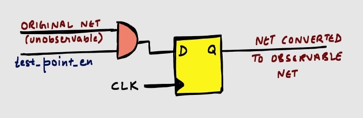
Observe Points:
An example of observe point inserted by Siemens’ Tessent tools is given in Figure 3. If test_point_en is ‘0’, the original_net’s value is blocked by AND gate as it will always output ‘0’. But if test_point_en is ‘1’, the AND gate output will be same as original_net, and it will be propagated to the flip-flop output to be observed.
It is evident from the above figures that adding TPs leads to extra logic, and hence more area. So, an optimum TP configuration is needed for efficient DFT testing. There are multiple configuration options provided by DFT tools, which are used while inserting TPs. These options allow DFT engineer to decide the number of TPs, type of TPs and even region of TPs. With some experimentation, optimum TPs can be decided and put into the design to get target coverage.

Leave a comment