There are a number of clock domains in modern day’s complex SoCs. When the flip-flops in such designs are stitched into scan chains, there is a possibility that there are two clock domains in one scan chain. This means that at one point in the scan-chain, the launch flop and capture flop will belong to different clock domains. This can lead to hold timing violation and cause issues in timing closure.
Hold Time Violation:
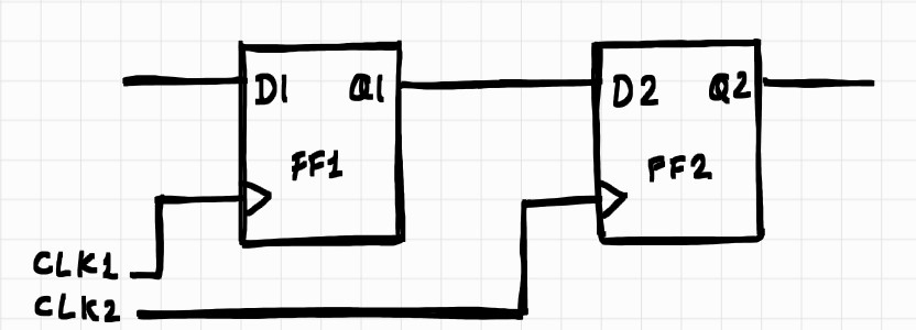
Figure 1 shows two flops connected in a scan chain, where CLK2 is delayed by a few nanoseconds than CLK1. The output of FF1 is connected to the input of FF2 directly.
The waveforms for the above circuit are given as follows:

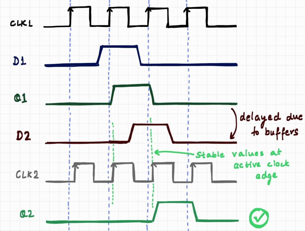
As we see, the D2 input changes within ‘hold’ time window for the flop FF2, and hence causing the metastability.
Buffer Insertion
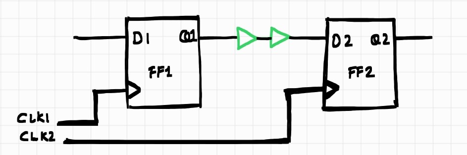
A simple solution to the above problem is, introducing delays in the data path by adding buffers. Let us see how that resolves the hold-time violation.
The waveforms for the circuit shown in Figure 3 are shown as follows:
However, the addition of buffers creates problems in closing timing across different Process, Voltage and Temperature corners. The more robust solution is a Lockup Latch.
Lockup Latch Insertion
Lockup latches are the sequential elements used to avoid hold time violations and handle clock skews in multi-clock domain designs, especially scan based designs where scan cells of two different clock domains are stitched together. Figure 5 is an example of two positive edge triggered flops (launch and capture) with a lockup latch inserted between them. This lockup latch is a negative latch and shares the clock with the launch flop.

The waveforms for the circuit shown in Figure 5 solve the problem of hold-time violation as shown in the waveforms below:
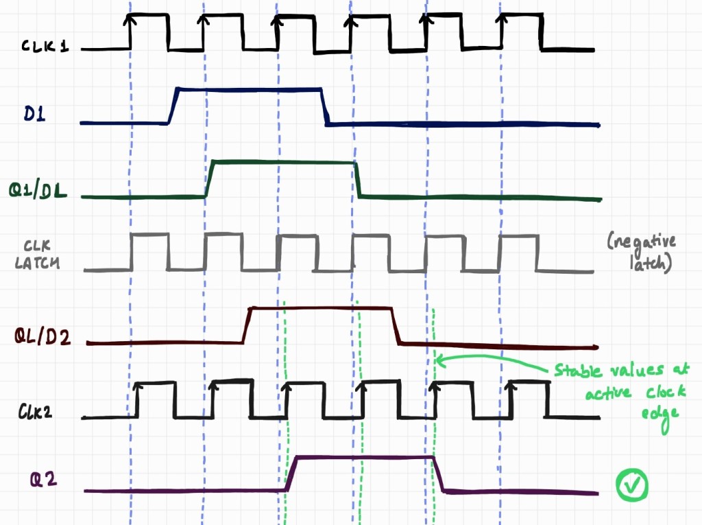
The negative latch holds the value and eases the hold time for the capture flop. Similarly, a positive lock-up latch can be used between two negedge clocks.

Leave a comment