DFT – ‘Design for Test’ is an important task in modern chip designs. Basic DFT constitutes scan design. I have discussed fault models and ATPG testing in different articles. Before going deeper into other DFT topics, let us understand what a scan design is.
When RTL design is coded and converted into gate netlist, the design consists of combinational and sequential logic. The sequential logic is formed by the registers (or flip-flops) in the design while the combinational logic is a collection of gates. The first step of making a chip design compatible for DFT/ Scan testing is converting each flip-flop into a scannable flip-flop. The scannable flip-flop looks as follows:
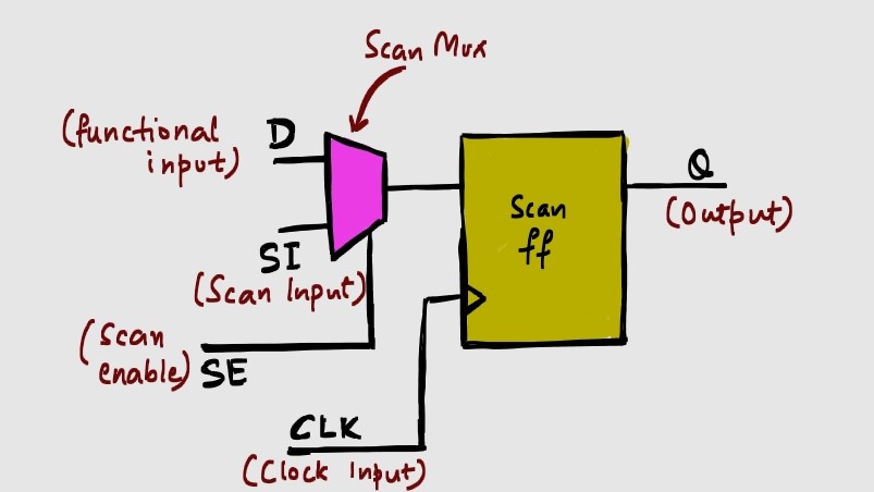
- A multiplexer is added with SE (scan_enable) pin as select pin
- One input to the multiplexer is the functional input (same as before). This value is propagated to the output when SE = 0.
- Other input to the multiplexer is Test input, through which a known value is assigned to the flip-flop. This value is propagated to the output when SE = 1.
The next step is connecting these scannable flip-flops together to form chains, called scan-chains. The number of scan-chains in the design is decided based on the
- number of scan flip-flops in the design and
- number of available ports in the design (for Scan-In and Scan-Out).
The output ‘Q’ of one scan flip-flop is connected to the SI input of next flip-flop.
There can be two scan modes:
Shift Mode (SE = 1)
The test input enters the scan chain through SI input of first flop and passes to the Q output. This Q output is directly connected to SI input of the second flop. As long as SE stays ‘1’, the test input keeps shifting into the scan flip flops.
Capture Mode (SE = 0)
The functional data from the combinational logic goes through D pin of the scan flip-flop and passes to the Q output of the flop. Every scan flip-flop captures the value from combinational logic this way.
Important points:
- ATPG helps to generate patterns for testing the manufacturing defects in the design, and is discussed in DFT-Fault Models.
- Scan clock is generally a slow clock, as testing is done at lower frequencies than the actual functional frequencies. At speed testing is done at functional frequency and is discussed in ATPG-Stuck-at and At-Speed.
- Not all flip-flops are converted into scannable flip-flops.
- As designs become larger, scan compression techniques are used to handle SCAN/DFT operations.
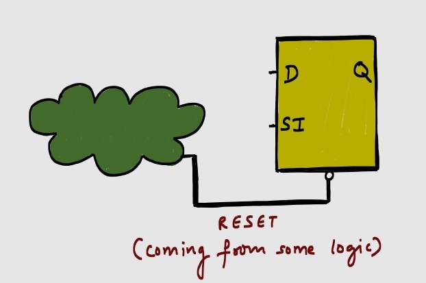
RESETs During Scan
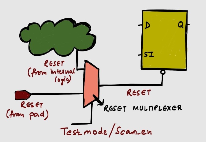
Resets are controlled separately in the scan design with the help of multiplexers.
When the patterns are shifted into, or out of the scan chain, scan chain is said to be in SHIFT mode. The requirement on RESET pin during shifting is that it should be de-activated/de-asserted. If the active value of RESET is ‘0’, it should be constrained to ‘1’ during the shifting. This is because an uncontrolled reset can affect the state of scan flip-flops, causing them to get in and out of reset unexpectedly. This disturbs the scan pattern data and hence, results in an incompetent DFT testing.
One of the simplest way of getting rid of this issue is using Reset Multiplexer. Reset multiplexer’s output provides reset to the scan flip-flops and is shown as:
- 0 input = Functional Reset
- 1 input = Controlled reset from the PAD
- SELECT input = TEST_MODE signal -> ‘0’ in functional mode and ‘1’ in Scan mode
So, whenever the circuit is in scan mode, the reset is directly coming from a pin (whose value can be easily controlled). This pin value can be constrained to ‘1’ for an active low reset, such that the circuit always remains out of reset in scan mode.
However, this leads to loss of coverage over functional reset paths. To avoid such coverage loss, the select signal of mux is a ‘scan_en’ like signal. The circuit then behaves as follows:
During Shift: ‘scan_en = 1’ -> Reset comes from the pin (controlled value)
During Capture: ‘scan_en = 0’ -> Reset value is obtained from functional reset which is allowed to toggle, and hence covered.
Alternatively, functional ‘reset’ signal can be muxed with a TDR (test data register) instead of a dedicated pin reset. TDRs are special registers, whose value can be controlled via IJTAG network. IJTAG is another DFT topic which will be discussed in further articles.

Leave a comment