Introduction to STA
There are certain timing specifications associated with the design, which are tested during ‘timing verification’. Timing is an integral part of chip designing and it basically separates a hardware and software code. It also determines the maximum frequency at which a design can operate.
Functional verification does not consider propagation delays and doesn’t verify any timing constraints. However, Timing verification includes all such delays. There are synthesis tools, which incorporate timing analysis. They use statistical estimates of delay, due to the resistance and parasitic capacitance of loading nets and interconnects in the design.
After the layout is finished, we can extract actual resistance and capacitance value, and hence delays. These values are back-annotated to match with the delay models generated by synthesis tools. In this way, a more accurate ‘post-layout’ timing analysis is done.
Examples of delays that are checked:
- Gate propagation delay
- Interconnect delay between gates
- Clock -skew
- I/O timing margins
- Device constraints (setup/hold/clock pulse-width)
There can be two kinds of timing verification:
Dynamic
Involves simulation of the behavior of the circuit to make sure that hardware constraints are met and design works according to performance specifications.
Needs test vectors.
Coverage is pattern dependent.
Long run times.
Heavy memory usage.
Might miss some checks as it is pattern dependent.
Limited to circuits with <1m gates.
Static
Involves analysis of all possible signal paths in the circuit to check if timing constraints are satisfied, without simulating the behavior of the circuit.
Does not need test vectors.
Coverage is pattern independent.
Comparatively smaller run times.
Light-moderate memory usage.
Might generate false alarms as a violation on a non-functional path can be reported.
Feasible for large circuits with millions of gates.
Based on the above points, Static Timing Analysis (STA) proves to be an efficient and more exhaustive way to be used for timing analysis. We will continue studying about STA from here. Since it is an extensive topic, we can break it down into bits. Let us revisit some terms that we will be using:
Critical path:
The longest path in the design which limits the speed at which circuit operates
Clock Path:
Path from a clock input port to the clock input of sequential element (flip-flop)
Load Capacitance:
The load capacitance of a gate is determined from the number of gates it is driving. If a gate can drive a maximum of 6 gates and a 7th gate is added, there will not be enough charge on each capacitor and the output of those gates might become ambiguous. Since the delays are determined using this load capacitances, it is important to understand these basics.
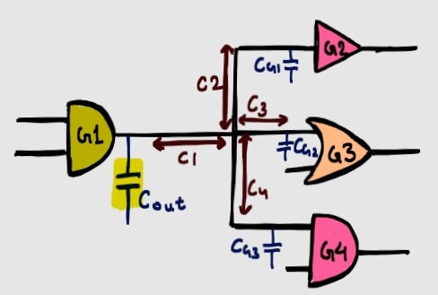
For example, the total load capacitance of gate ‘G1’ in the following figure is:
Cout = C1 + C2 + C3 + C4 + Cg1 + Cg2 + Cg3
Cout = Cwire + Cg1 + Cg2 + Cg3
CMOS Switching:
The ideal output of a CMOS inverter is:
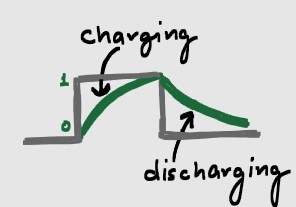
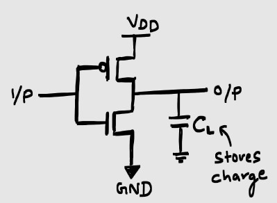
However, the actual switching happens by charging and discharging the load capacitor. This takes time and the actual waveform is represented by the ‘green’ lines in the Figure 2.
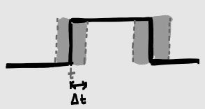
Clock Uncertainty:
If the clock reaches a flop at time ‘t’, it is not important that the clock will reach in exact same time in the next clock cycle. In next cycle, it may reach in a little less or little more time, within a small range ‘$t’. This window is called ‘clock jitter’ and the clock uncertainty can be given as:
U (Uncertainty) = t + $t
Clock to Q delay:
It is the time taken by data to reach the output of the flop, from the time when clock triggers.
Combinational Delay:
The time between the change of an input (of a combinational circuit) until it reaches the output is called combinational delay. These include the propagation delays due to the load capacitance and switching, as we studied earlier.
What STA does?
A simplified way of understanding what STA does is:
- Break the design into timing paths
- Calculate signal propagation along each path
- Check for timing violations
We will learn about Timing paths in second phase of this article

Leave a comment